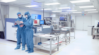
APX300 (S option) is a dry etching equipment specialized in compound/non-volatile material processing, which can handle wafers from ⌀2" to 8" and odd-form PCBs. Two types of transfer methods can be selected. (Atmospheric transfer and vacuum load lock)
Features
- Two types of plasma sources support high-speed and high-accuracy processing
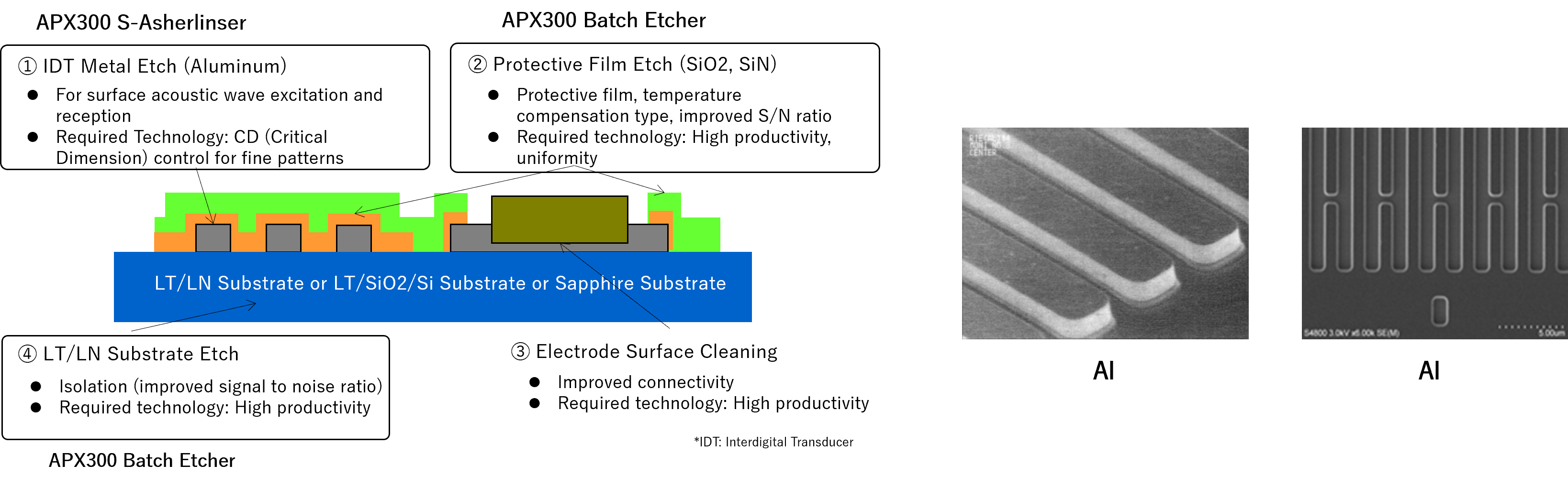
Enables high-speed deep hole drilling of compound materials (through-PCB) and processed film thickness control - The addition of an usher chamber and rinse chamber enables metal processing without residue or corrosion
- Stable processing of non-volatile materials by an in-situ top plate deposit removal function
Application
- Power devices, SAW, communication devices, MEMS, sensors
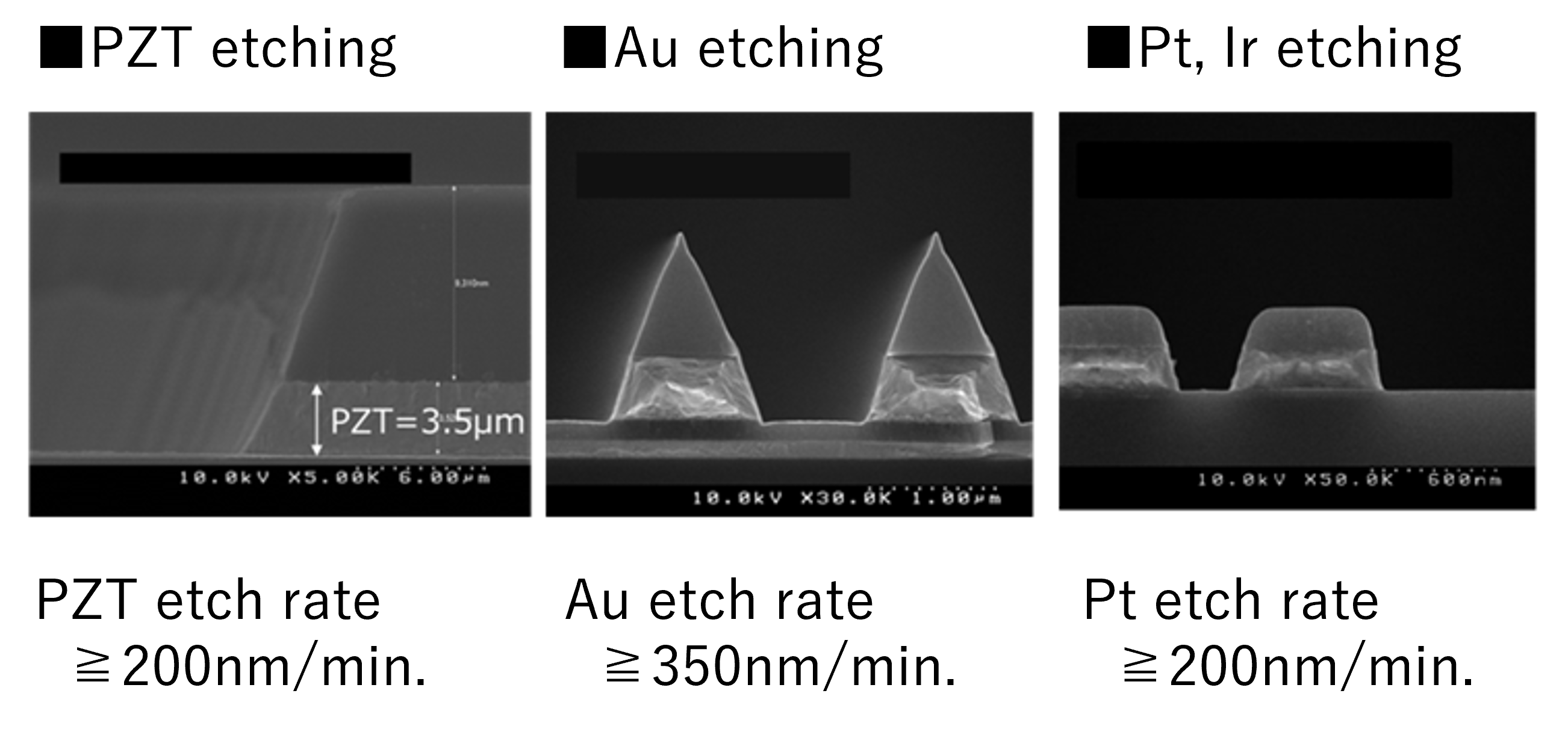
(SiC, GaN, GaAs, Al, Au, Pt, PZT, etc.)

Key features and functions
- Two types of plasma sources enable high-speed and high-precision machining
Achieves high-speed deep drilling of compound materials (substrate penetration, etc.) and control of processed film thickness - Achieves metal machining without residue and corrosion by adding usher and rinse chambers
- In-situ garment removal function with top plate enables stable machining of non-volatile materials
The APX300 (S option) is a dry etching system specializing in the processing of chemical compounds and non-volatile materials. It is compatible with wafers of 2 inches to 8 inches and irregular substrates, and two transport methods can be selected: “Atmospheric loading supply ” and “ Vacuum load lock supply ” CE certificated.
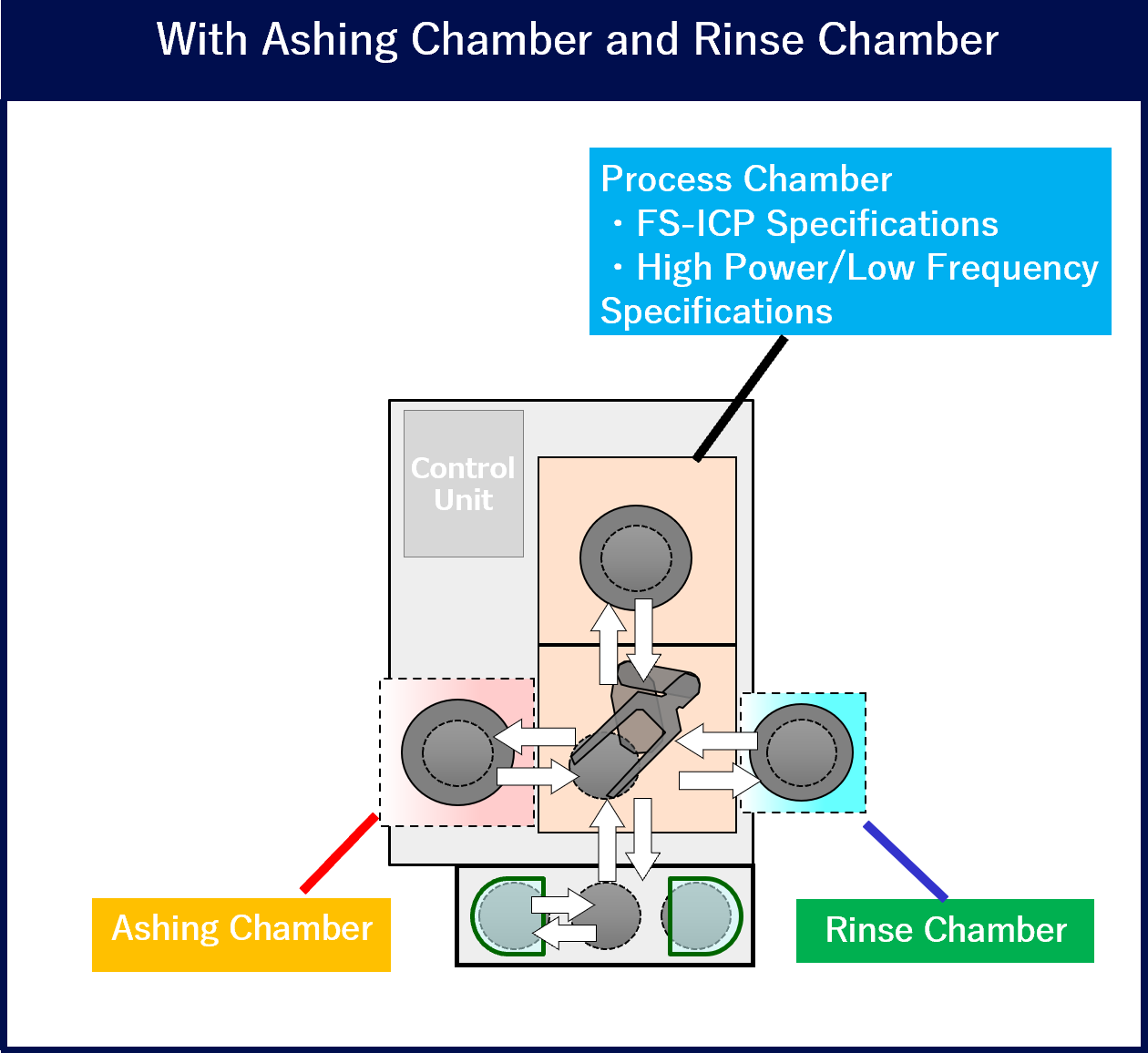
This equipment is a single-wafer processing type for wafers of 8 inches or smaller, and can be selected and optimized for a wide range of process applications such as power semiconductors, optical communications, high-frequency communications, RF modules, and MEMS.
In addition, as a post-etching process, the ashing and rinsing chambers can be expanded according to the process application.
Extended specifications with ashing and rinse chambers enable anticorrosion treatment during metal processing.
- Ashing chamber:
Supports high/low temperature/H2O ashing
Resist ashing treatment, dechlorination/defluorination anticorrosion treatment - Rinse chamber:
In-line cleaning (pure water, * chemical solution) prevents corrosion that is difficult to control by ashing

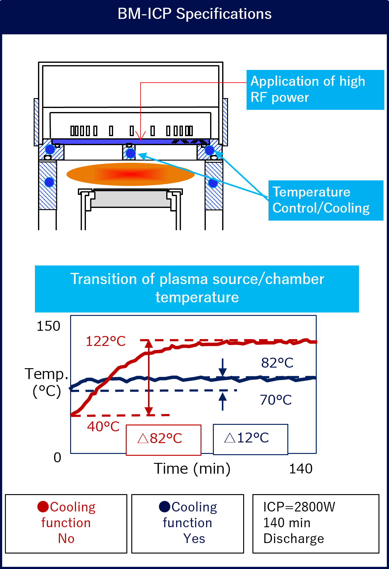
High-density plasma and chamber temperature control (top plate and side wall) provide stable high-speed processing
- High-density plasma source capable of applying high power
- Cooling and temperature control of plasma source and chamber side wall stabilize temperature and suppress thermal damage to wafer
FS-ICP enables stable machining of non-volatile materials by removing garments attached to the top plate
※Corrosion protection is possible with extended specifications (Ashing and Rinsing Chambers)
- FS-ICP Plasma Source:
FS antenna directly under the ICP coil removes deposits attached to the top plate, enabling longer maintenance cycle (cleaning frequency: less)
RF applied independently to ICP and FS
Control Achieves wide process window and stability - Ashing/Rinsing Chambers:
In-line ashing/rinsing prevents resist removal and chlorine/fluorine corrosion

By applying radio frequency (RF) to the FS antenna and sputtering the top plate, it is possible to suppress and remove unnecessary deposits from the top plate.
In addition, by generating high-density plasma and maintaining stable plasma during mass production of non-volatile materials, long-term MTWC is realized.
About Dry Etcher
Examples of LED and power devices, and communication devices and MEMS and sensors
Information on current seminars and exhibitions is compiled and posted here. Information on past seminars and exhibitions is also available.
