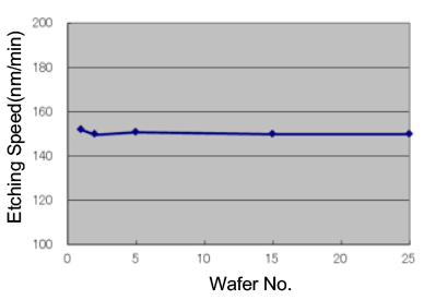
- Need to achieve high productivity
- Need to achieve increased brightness of LED
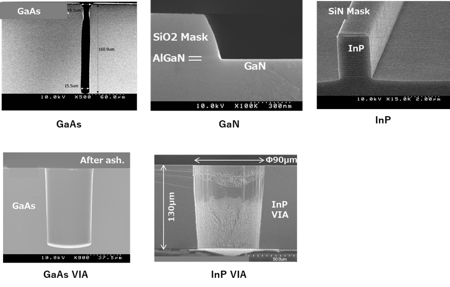
- Need to achieve high resolution processing of compounds
- Need to perform etching of non-volatile materials
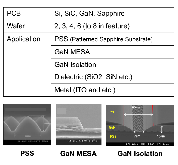
▲Examples of utilization and application of various materials

| Classification | Single wafer/batch type dry etcher | Single wafer type dry etcher |
| Model |
APX300 |
APX300-S |
|---|---|---|
| Exterior | Housing multiple devices in one box increases the area productivity |
The E620 process chamber with extensive track record is bonded on the latest APX300 platform |
| Features |
|
|
| Target wafer | Multiple wafers Batch treatment (tray specification) |

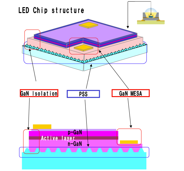
▲Case studies of application and processing of LED
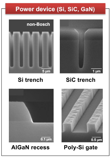
LED and power device application case studies
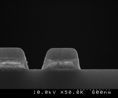
Low-damage and high-speed processing of GaN contributes to high productivity in LED electrode formation/element separation processes
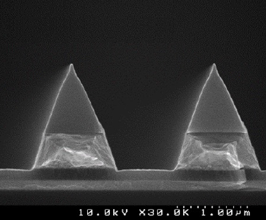
PSS (Patterned Sapphire Substrate) processing contributes to increased brightness of LED elements
Supports batch treatment of multiple sheets of φ2, 4, 6 inch wafers
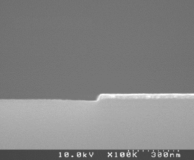
Realizes high-resolution processing that matches every need of next generation power devices
| SiC power device, SiO2 mask etching |
SiC power device, SiC trench etching |
|---|---|
| Si power device, Si trench etching | SiC power device, SiC recess etching, Poly-Si entire surface etch back |
▲Case studies of application and processing of power devices

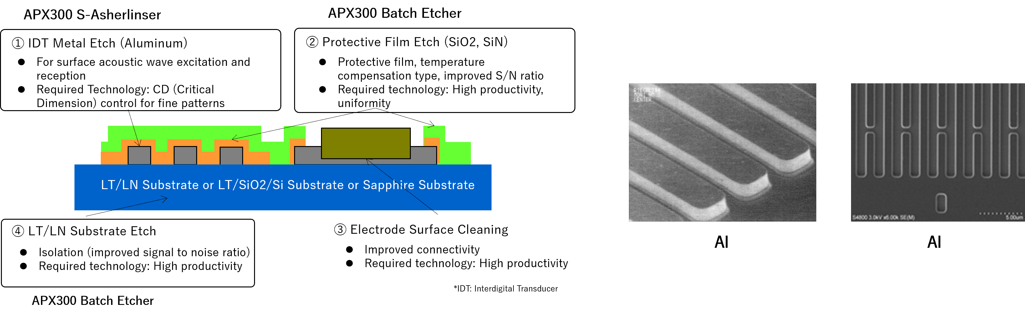
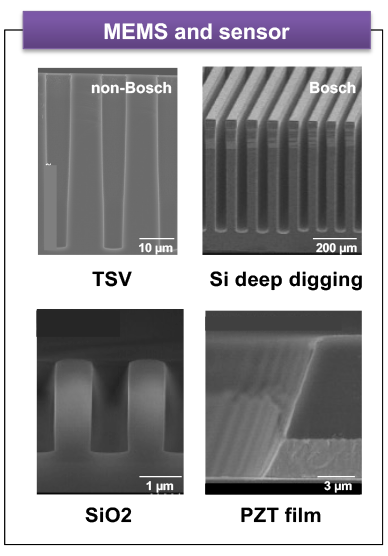
Processing of dielectric films, metals, and silicon used in gyroscopes, pressure sensors, printer heads, etc.
■Piezoelectric MEMS, PZT thick film etching (FS-ICP plasma source application)
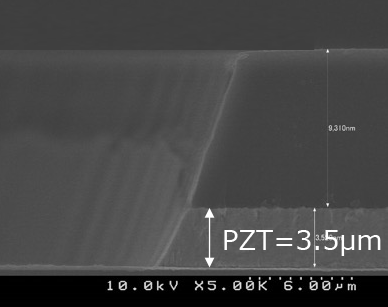
PZT E/R ≧ 50 nm/min
Uniformity
In wafer ≦ ±5%
W to W ≦ ±1%
PR selectivity ≧ 0.7
Pt selectivity ≧ 8
■Non-volatile material etching (FS-ICP plasma source application)
E/R ~100nm/min.
Unif. ≦ ±5%
PR Sel. ≧ 0.6~1.5
No fence, No corrosion
E/R ≧400nm/min.
Unif. ≦ ±5%
PR Sel. ≧ ~2.0
No fence
E/R ≧200nm/min.
Unif. ≦ ±5%
HM Sel. ≧ 10
No fence
E/R ≧140nm/min.
Unif. ≦ ±5%
0.4um L/S
No fence
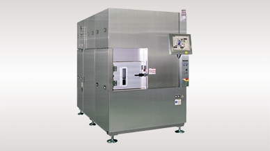
Dry Etcher
APX300
Housing multiple devices in one box contributes to increase in area productivity.
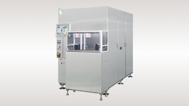
Dry Etcher
APX300 (S option)
The E620 process chamber with extensive track record is bonded on the latest APX300 platform.
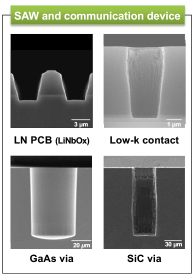
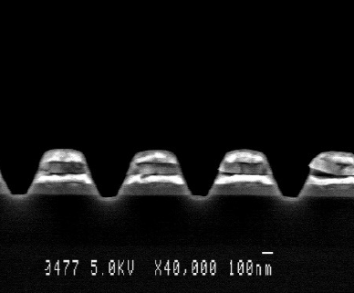
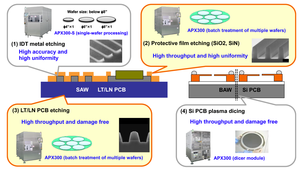
Realization of high resolution processing of IDT (interdigital transducer) and various metals
Achieves high productivity by batch etching of multiple wafers with thick oxide film or LT/LN wafers
High speed and deep etching process of compound PCB (GaAs via, SiC via, Si via)
GaAs scribe and dicing process
▲Case studies of application and utilization of each material
Etching of various materials (Piezo, Non-volatile, Si) such as the gyro, pressure sensors and printer head
▲ Case studies of application and processing of each material