Campaign bands
Background colour
White
Section intro title
Do you face any of these problems?
Anchor link ID
PlazmaDicer-01
Band body
- Need to eliminate damage and chipping
- Need to achieve high productivity by batch treatment with plasma
- Need to suppress the occurrence of dust/particle that causes lower yields
- Need to design chip shapes freely
Background colour
Grey
Section intro title
Plasma dicer realizes high productivity by damage-less and clean dicing.
Anchor link ID
PlazmaDicer-02
Column items
Column body
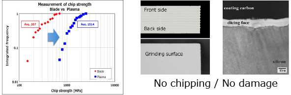
- Damage-free, chip-free and improved die strength of chip
- Thin wafer (≦50 μm) can be separated into pieces with low damage
- Capability that helps to separate into pieces with low device damage
Media
Media
Column title
1. No damage and no chipping
Column body
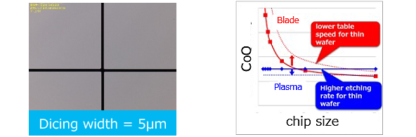
- Batch process treatment and high Si processing speed
- Narrow dicing widths (≦5 µm) and narrow kerf margins achieved by chipping or cracking allowing for more chips per wafer
Media
Media
Column title
2. High productivity and low CoO
Column body
- Chemical reaction processing by plasma etching, a clean process free from mechanical damages that generates mechanical dust, vibration and water pressure
- Capability to improve yield
- Potential to reduce the number of inspections and inspection points
Media
Media

Column title
3. Dust-free and particle-less
Column body
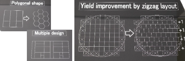
- No restrictions of chip shapes and layouts other than a grid
Media
Media
Column title
4. Various chip shape and layout support
Background colour
White
Section intro title
Target machinery and target packages
Anchor link ID
PlazmaDicer-03
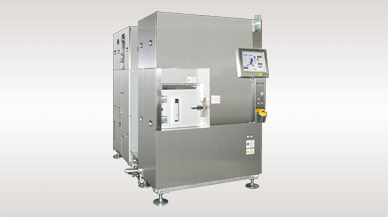
Wysiwyg body
| Model |
APX300-DM |
|---|---|
| Exterior | Realizes damage free, takes more chips and improves productivity with the plasma dicing technology |
| Features |
|
| Target wafer |
Background colour
Grey
Section intro title
Solutions
Anchor link ID
PlazmaDicer-04
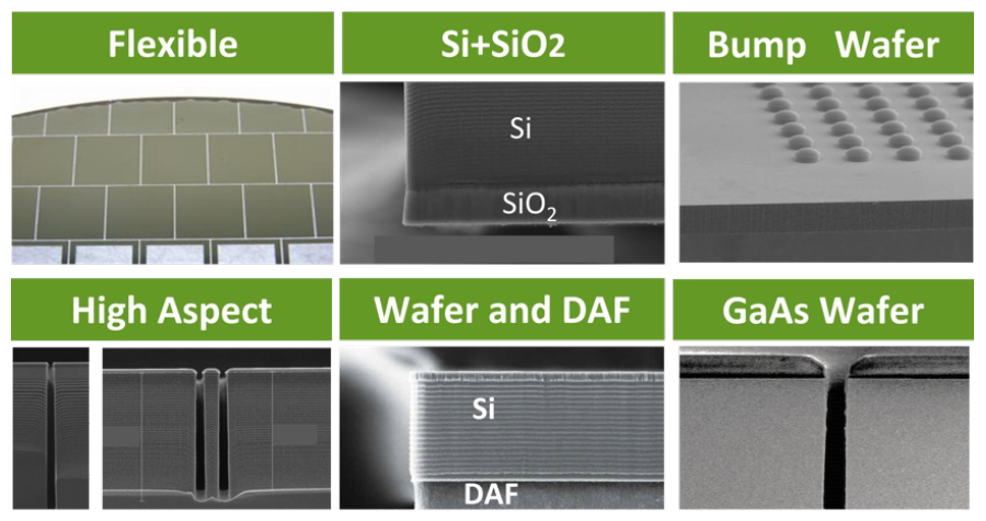
Band intro title
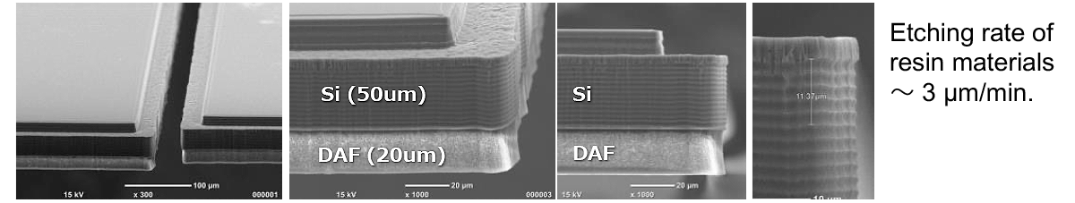
Plasma dicing of plastic materials like DAF
Band body
▲Process case study
Media
Media
Band intro title
Plasma dicing of laminated wafer such as insulated film and WoW structure
Media
Media

Band intro title
Various other case studies of processing
Media
Media
Band intro title
Related products
Column items
Column body
Plasma Dicer
APX300-DM
Reduces damages, takes more chips and increases productivity with the next generation plasma dicing technology.
Media
Media
Background colour
White
Section intro title
Inquiries
Anchor link ID
PlazmaDicer-05
Wysiwyg body
URL alias
/products-services_fa/solutions/device-related/plazma-dicer
Use WYSIWYG header
On
Campaign header WYSIWYG
Plasma Dicer [Solution]
Automate carousel?
Off