Campaign bands
Background colour
White
Section intro title
Demonstration centers for semiconductor-related systems (Toyonaka and Minoshima)
Anchor link ID
Kadoma-01
Band body
We have the necessary devices for evaluation, and inspection devices for demonstration to obtain accurate results, and we accept demonstration requests from customers.
Column items
Column body
Media
Media
Column body
Media
Media
Background colour
Grey
Section intro title
Device and demonstration support details
Anchor link ID
Kadoma-02
Item body
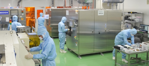
Toyonaka site [Plasma dicing demonstration center]
Support details:
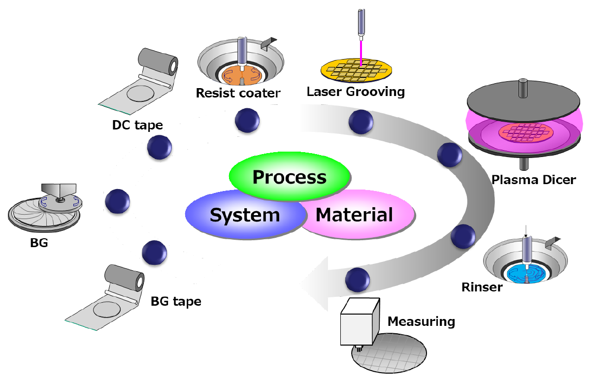
Demonstrations of plasma dicing for silicon wafers with a diameter of 200 mm or 300 mm
(Wafers with a size of 200 mm or less are also supported)
Main devices:
- Plasma Dicer APX300-DM
- Peripheral processing devices
- Back grinder:
Thins wafers to a specified thickness - Lithography:
Applies a protective layer of plasma irradiation to the wafer to determine the dicing position - Laser patterning:
Forms dicing lines
- Back grinder:
- Inspection devices
Measurement of processing steps and film thickness, electron microscopy, etc.
Media
Media
Item body
We have all the necessary devices for processes before and after plasma dicing to provide a one-stop demonstration service.
Media
Media
![Kadoma site [Dry etching demonstration area]](/sites/default/files/2022-03/fa-campaign-showroom-kadoma-04.png)
Item body
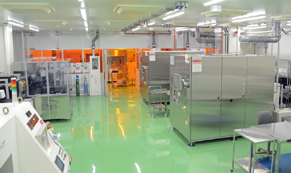
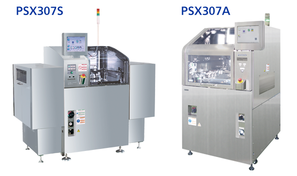
Toyonaka site [Plasma cleaning demonstration area]
Support details:
Effectiveness of plasma cleaning PCBs and wafers
Main devices:
- Plasma Cleaner PSX307S, PSX307M, PSX307A
- Inspection devices
Water droplet contact angle measurement, surface elemental analysis, film thickness measurement, electron microscopy, etc.
Media
Media
Item body
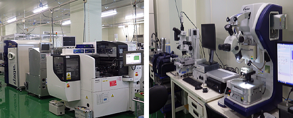
Minoshima site [Die and flip-chip bonding demonstration area]
Support details:
Die bonding and flip-chip demonstrations
Main devices:
- Die Bonder MD-P200DA
- Flip Chip Bonder MD-P200US2, MD-P300
- Inspection devices
Transmission X-ray device, die shear tester, metallographic microscope, etc.
Media
Media
Background colour
White
Section intro title
Location
Anchor link ID
Address
Column items
Column subtitle
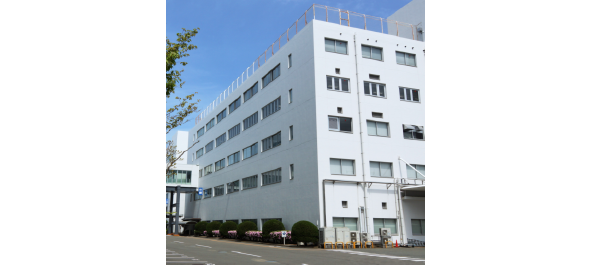
Toyonaka site
Column body
1-1-3, Inazucho, Toyonaka City, Osaka 561-0854
Media
Column subtitle
Minoshima site
Column body
4-1-62 Minoshima, Hakata-ku, Fukuoka City, Fukuoka 812-8531
Media
Band body
For details, please contact one of our sales companies or sales representative.
Alternatively, please use the Inquiry Form at the bottom of this page to contact us.
Background colour
Grey
Section intro title
Inquiries
Wysiwyg body
URL alias
/products-services_fa/supports/showroom/kadoma
Use WYSIWYG header
On
Campaign header WYSIWYG
Demonstration centers for semiconductor-related systems
Automate carousel?
Off
Display in-page navigation
Off
Header Type
wysiwyg_header